On mapping DSP algorithms into FPGAs
Engineering Simulation, Gordon Breach Publ. Group. − V. 18. −2001. − P. 217−225.
On mapping DSP algorithms into FPGAs.
Anatoli Sergyienko National Technical University of Ukraine “KPI”, Kiev, Ukraine,
Juri Kanevski Technical University of Koszalin, Koszalin, Poland,
Roman Wyrzykowski Technical University of Czestohowa, Czestohowa, Poland
The problem of mapping digital signal processing (DSP) algorithms into application specific structures, especially into field programmable gate arrays (FPGAs) is considered. A new mapping method is proposed which takes into account structural properties of FPGA, minimises its hardware volume, and provides designing pipelined structures with high clock frequency. This method was tested by designing infinite impulse response (IIR) filter structures which are implemented in FPGA. The filter structures are described by VHDL and have high throughput and hardware utilisation.
1. Introduction.
DSP applications are characterised by real time computations of data flows using calculation intensive algorithms with minimum condition operators. Many of them, for example, in the video digital signal processing domain, have high throughput which is derived by quantisation frequency fQ of tenths megahertz. Therefore, such applications are usually heavily pipelined solutions, and are implemented in ASICs. Often they are implemented in FPGAs, which technology supports high clock frequency fC which is equal to tenths and hundreds megahertz, small time period and cost of application development. But they have a set of structural properties and constrains which must be taken into account by designing cost effective DSP applications with high throughput.
Consider such an application in Xilinx FPGA. It must be heavily pipelined, because, one hand, complex logic is performed by a chain of lookup tables, and therefore, without pipelining it is impossible to get the proper performance, the other hand, one bit pipeline registers can be attached everywhere in the structure without additional cost. The cost of four input multiplexor is approximately equal to an adder cost. Therefore, the multiplexor input number must be carefully minimised as well as adder number must be. The number of programmed wires in FPGA is enough for many applications but is still limited to prototype randomly connected units. Besides, the long line delay is equal to the logic unit one. Therefore, the local interconnections and its pipelining are preferable.
Many approaches of algorithm mapping have been published that are tailored to DSP application domain that differ both in synthesis tasks and in target architecture. Examples are CATHEDRAL system targeting bit sequential computations or microprogrammable bidirectional bus architectures [1], PHIDEO system, tailored to video applications [2], Sehwa system targeting pipelined structures, HAL system which assumes multiplexor oriented structures [4]. Most of such systems intended for automatic ASIC design like silicon compiler, and are not targeting FPGAs. Besides, optimisation demands to FPGA projects are more strict than ones to ASICs due to restricted place and route possibilities of FPGAs.
In this paper a new method for mapping DSP algorithms into application specific processor is proposed which takes into account structural properties of FPGA, minimise its hardware volume, and provide designing pipelined structures with high clock frequency.
2. Method for mapping data flow graphs into application specific structure.
The mapping method compendiously described below is well suited for mapping DSP algorithms into application specific structures and was published in [5,6,7]. In this paper it is adapted to FPGA applications. Often DSP algorithms are described by data flow graphs (DFG). In DFG operator nodes represent operations of addition or multiplication, a chain of k delay nodes represents delay of a signal variable to k iterations, edges represent data flows. DFG can be derived by respective mapping of reduced dependence graph GAR of an unimodular loop nest [8]. In the graph GAR nodes represent operators, and weighted by k edge represents dependence of the data which is delayed to k iiterations.
Both DFG and reduced dependence graph GAR can be represented in n-dimensional space Zn. For most DSP algorithms it is enough to operate with n=4 dimensional space. Each of N nodes of the graph which denotes the algorithm operator is represented by the vector – node Ki, i=1,…,N. The coordinates of the vector Ki signify iteration number, clock number in the iteration, processing unit (PU) in which the respective operator is implemented, and its type. Each of M edges of the graph which denotes the data dependence or variable moving is represented by the vector – edge Dj = Ki – Ki-1, j=1,…,M, besides, vector DN+1 = K1.
Sets of vectors Ki and Dj form respective matrices K and D which together with the graph GAR incidence matrix A form an algorithm configuration CA = (K,D,A). The configuration CA is equal to the composition of structure configuration CS = (KS,DS,A) and configuration of events CT = (KT,DT,A), namely
K = (KST, KTT)T; D = (DST, DTT)T
where vector-node KSi ∈KS, represent coordinates of PU where i-th operator is implemented, vector-edge DSj ∈DS represent relative coordinates of communication line for j-th variable, vector-node KTi ∈KT represent clock period of this operator implementation and vector-edge DTj ∈DT represent delay of this variable moving. Another words, configuration CS represents the graph of the processor structure, and the configuration CT represents the operator time schedule.
The following definitions and statements are true for configurations CA, CS, CT. The configuration CA is correct if Ki ≠ Kj ; i,j = 1,…,N, i≠j, i.e. all of vectors-nodes are placed in the space separately.
There is a linear dependence between matrices: D = KA; K = DoAo-1, where Ao is the incidence matrix for the maximum spanning tree of the graph GAR, and Do is the matrix of vectors-edges of this tree.
Correct configuration CA can be transformed into equivalent configuration CA’ by any injection function. For example, the following transformations give equivalent configurations: permutations of vectors Ki, multiplications of the matrix K and non-singular matrices P.
The sum of vectors-edges Dj ,which belong to any loop of the graph GAR must be equal to zero. The configuration CT is correct if Dtjge;0, where Dtj is unweighted dependence vector of the graph GAR, inequality has lexicographic meaning, j =1,…M. Besides, the given algorithm is implemented in pipelined manner correctly iff
∀KTl∈KT(KTl=(i,q)T, q∈(0,1,…,L-1)), (1)
where KTi is not incident to edge DTj=(p,0)T weighted by p, L is the period of time between two consecutive loadings of the same input operand or latency of the algorithm implementation.
Searching for algorithm mapping consists in deriving configurations CA, CS, CT which are optimised according to given criterion. Directed searching for optimised configurations is implemented taking into account mentioned above definitions, dependencies and constraints.
At the first stage of the mapping, the searching for the space component CS is implemented. The forming of the matrix KS consists of distributing Mk operators of the k-th type among ]Mk/L[ processing units of the k-th type. As a result, MS groups of equal columns are formed in the matrix KS , where MS is the number of PUs in the resulting structure. The goal of this process is resource allocation and resource assignment.
At the second stage, the time component CT of the mapping is searched for. Derived matrices KT and DT must satisfy the condition of algorithm configuration correctness, correctness of the configuration of events, condition, that the sum of vectors-edges Dj ,which belong to any loop of the graph GAR must be equal to zero , and condition (1). Besides, if the operator represented by KTl is calculated for d clock cycles, then the norm R(DTj)=iL+q of the vector DTj=(i,q)T must be no less than d. The clock period in which the operator represented by KTl=(i,q)T is implemented is equal to t = R(KTl). As a result, the operator schedule is derived.
In a large set of different exemplars of mapping results an optimum mapping is searched. Some heuristics can be applied to derive a quick solution, such as list scheduling, force directed scheduling, loop folding, or left – edge algorithm, etc. [9]. The advantages of this method consist in the following. Both stages of the mapping deriving can be executed in different order or simultaneously providing best optimisation strategy by time constrained scheduling and functional pipelining. The pipelined PUs with the given stage number can be taken into account. After some adaptation this method is well suited for mapping algorithms into FPGAs.
3. Method for mapping data flow graphs into FPGA.
The main significant PU type for DSP applications are adder and multiplier. Due to FPGA properties, these type PUs must be pipelined and have minimum input wires. Accumulator and pipelined multiplier to the coefficient correspond to these demands. The accumulator has one input and consists of an adder with register. The pipelined multiplier represent the combinatorial multiplying network which is divided by pipeline registers to d stages with approximately equal delay. When this delay is equal to the adder one, the high throughput rate is achieved.
To synthesise the structures with accumulators and pipelined multiply units as well as to minimise the register and multiplexor input numbers the third stage is introduced to the method described above. This stage is executed after first and second ones. In this stage the additional delay nodes and adder type nodes are introduced to edges of the DFG and graph GAR which do not alter the algorithm.
The introduced delay nodes which are represented by vectors KDi are mapped into registers. The vectors-edges Dj which are incident by its begins to vectors-nodes KDi must be mapped into one clock cycle delay, i.e. R(DTj)=1.
The vectors-edges Dj which are incident by its begins to vectors-nodes KMi, which represent multiply operation must be mapped into d clock cycle delay, i.e. R(DTj)=d. The delay nodes are not introduced to these vectors-edges. By posterior mapping vectors-nodes KMi, d staged multipliers are gained.
The additional adder type nodes are introduced to vectors-edges Dj which are incident by its begins to adder type vectors-nodes KAi , and which are mapped into several clock cycle delay, i.e. R(DTj)>1. As a result, chains of up to L-1 adder type nodes are gained, which are mapped into the accumulator type PUs. Besides, the additional adder type node is introduced to vector-edge Dj (R(DTj)>1) which is incident by its end to vector-node KAi which is the first in the chain of adder type nodes. This assures mapping addition operators into the accumulator type PUs with a single input.
Finally, the stage of the searching for the space component CS is implemented again. By this process the number of both multiplier, accumulator PUs and registers is minimised more precisely in a sigle stage and this fact testify the advantages of this method.
4. Example of the synthesis.
Infinite impulse response (IIR) filters are widely used in digital signal processing systems because they have computational complexity several times as less as finite impulse response filters have. Implementation IIR filters in FPGA has a set of advantages, such as full adaptation of implemented in FPGA structure to the filtering algorithm, high throughput, hardware utilisation effectiveness, achieving high rate of calculating precision. But due to the feedback chains in IIR algorithms such popular methods of algorithm optimisation like retiming and pipelining give limited results. In the case when the clock frequency fC is L=2,3,… times as much as the quantisation frequency fQ of the digital signal is, there are a wide opportunity to enlarge pipelining of IIR filter calculations, and therefore to derive filter structures which support maximum hardware utilisation and high clock frequency when implementing in FPGA.
Consider the second order all pass IIR filter design. It calculates the following difference equations yi=xi+c1yi-1+c2yi-2; vi= c2yi+c1yi-1+yi-2, where xi are initial dates, vi are results, and c1,c2 are filter coefficients.
The DFG of this filter is illustrated by the fig1.
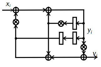
Here rectangles represent registers, circles with plus sign and with cross sign represent addition and multiplication operators, respectively. Consider the resulting structure which contains d=2 staged multiplier PUs and one input accumulators. According to the rule that the minimum time period of one algorithm iteration is equal to maximum sum of delays in separate loop of DFG, divided by the register number in it [9], this time for the given algorithm is equal to sum of one multiplier delay and one adder delay. Taking into account that one multiplier delay is approximately equal to two adder delays, it is recommended to consider the latency period be equal to L=3 clock cycles. This assures deriving the structure with maximum throughput and minimum cost.
Then first and second stages of the filter structure synthesis are implemented. The resulting optimised algorithm configuration CA is illustrated by the fig.2.
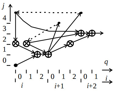
Here coordinates i, q, j represent iteration number, clock cycle in the iteration, and PU number, respectively, the dotted lines represent edges weighted by the factor one and two which correspond to delay the variable yi to one and two iterations. This configuration is mapped into the filter structure which consists of one multiplier unit, two adders, and nine registers.
After executing the third stage of the synthesis the optimised algorithm configuration CA’ is derived, which is illustrated by the fig.3.
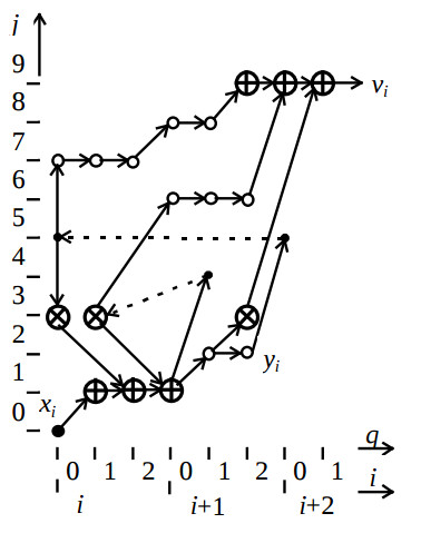
Here small circles represent additional delay nodes. The respective structure configuration CS is shown on the fig.4.
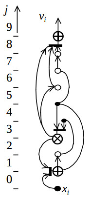
It represent the structure graph which can be derived by connecting together the vectors-nodes on the fig.3 which have equal coordinates j. The bold lines on the fig.4 represent respective multiplexers. The resulting structure is shown on the fig.5.
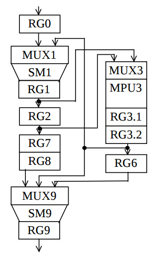
Its hardware cost consists of one pipelined multiplier, two accumulators, three multiplexers and nine registers, and is minimum for the given latency L. After third stage of the synthesis the number of multiplexers and their inputs in the target structure is decreased by one. When multiplier is designed as a scaler then the clock period is equal to the sum of delays in the multiplexor, adder and register, and can achieve the minimum clock period which afford FPGA.
5.Conclusion .
Implementation DSP algorithms in FPGA has a set of advantages, like full adaptation of implemented in FPGA structure to the algorithm, high throughput, hardware utilisation effectiveness, any rate of calculating precision. The DFG of the signal processing algorithm is mapped into the application specific structure. But due to the feedback chains in many DSP algorithms like in IIR filtering ones such methods of algorithm optimisation like retiming and pipelining give limited results. Most of known mapping methods intended for automatic ASIC design, and are not targeting FPGAs. Besides, optimisation demands to FPGA projects are more strict than ones to ASICs due to restricted place and route possibilities of FPGAs.
In this paper a new method for mapping DSP algorithms into application specific processor is proposed which takes into account structural properties of FPGA, minimises its hardware volume, and provides designing pipelined structures with high clock frequency. The method is based on the representing DFG in multidimensional space with time, resource number, operation type coordinates and its mapping into subspaces of structures and events. Searching for the optimised structure is implemented by the linear algebra and linear programming methods or by another approaches. The operator sheduling and allocation are performed implicitly and simultaneously by the direct searching and therefore the optimisation process has decreased complexity. The register allocation is performed simultaneously with another resource allocation, which assures the maximum hardware utilisation effectiveness.
Some heuristics direct the mapping to implement pipelined processing units like multipliers and accumulators, that is preferable for FPGA. Derived structures are operating in pipelined regime providing high hardware utilisation effectiveness and minimised clock cycle period.
This method has showed good results by the development of the library of IIR filter structures. The development and mapping of algorithm configurations was held by means of a framework Paredit which is described in [7]. The library contains a set of parametrised IIR filter structures and is intended to computer aided design of digital signal processing systems on the base of FPGAs. The structural parameters are filter order and latency L. The library consists of structural models of filters described by VHDL language in synthesable style, and therefore can be translated both into FPGA of any type and into ASIC using such synthesis tools like Synopsys.
References
1. J. Rabaey, H. de Man, J. Vanhoof, G. Gossens, F. Catthoor, CATHEDRAL-II: A Synthesis System for Multiprocessor DSP Systems, In D.D.Gajski , ed., Silicon Compilation, Addison-Wesley, 1988, pp. 311-360.
2. P. E. R. Lippens, J. L. van Meerbergen, A. van der Werf, W. F. J. Verhaeght, PHIDEO: A Silicon Compiler for High Speed Algorithms, In Proc. European Design Automation Conf. (EDAC), pp. 436-441, 1991.
3. N. Park, A. C. Parker, Sehwa: A Software Package for Synthesis of Pipelines from Behavioral Specifications, IEEE Trans. CAD, 1988, V.7, N.3, p.356-370.
4. P. G. Paulin, J. P. Knight, Scheduling and Binding Algorithms for High-Level Synthesis, In Proc. 26-th ACM/IEEE Design Automation Conf. (DAC), 1989, p.1-6.
5. J. S. Kanevski, A. M. Sergyenko, H. Piech, A method for the structural synthesis of pipelined array processors, In Proc. 1-st Int. Conf. on Parallel Processing and Applied Math. – PPAM’94. Czestochowa (Poland), 1994, pp.100-109.
6. Yu. S. Kanevskiy, L. M. Loginova, A. M. Sergienko, Structured Design of Recursive Digital Filters, Enginering Simulation, 1996, V.13, pp. 381-390.
7. A. Sergyienko, A. Guzinski, Ju. Kanevski, A method for mapping unimodular loops into application specific parallel architectures, In Proc. 2-nd Int. Conf. on Parallel Procesing and Applied mathematics. PPAM’97. Zacopane, Poland, Sept. 2-5, 1997, p. 362-371.
8. VLSI and Modern Signal Processing, Ed. by S.Y.Kung, H.Whitehouse, T.Kailath, Prentice Hall, 1985.
9. The Synthesis Approach to Digital System Design, Ed. by P. Michel, U. Lauther, P. Duzy, Kluwer Akcademic Publishers, 1992.