Minimized FIR Filter Design Implemented in FPGA
Vinogradov Ju. N., Sergiyenko A. M., Quadir S. H.
Computer Engineering Department of NTUU “Igor Sikorsky Kyiv Polytechnic Institute”, Kyiv, Ukraine
Introduction. The field programmable gate array (FPGA) is widely used for the high-speed digital signal processing. FPGA architecture is adapted for the effective finite impulse response (FIR) filter implementation. For this purpose the Xilinx FPGAs contain the DSP48 blocks, each of them is intended for a single filter stage calculation in the pipelined mode. But the filter length is limited by the FPGA volume and by the number of the DSP48 blocks in a single column of the chip. So, the length of the FIR filter which is generated by the Xilinx Coregen tool for the Spartan-6 devices is limited by the numbers from 8 to 48 [1]. And the more this number the more expensive the chip is. Besides, when FPGA is used only for the filtering, then the configured hardware like look-up tables (LUTs), registers is underloaded and is used ineffectively.
There are many methods of the multiplier-less FIR filter implementation. The most of them use the constant coefficient multipliers (CCMs), which have the minimized hardware volume. They are widely used in FPGAs for decades. But no one of them uses the hardware multipliers like the DSP48 block [2–4]. In the presentation, a new method of the FIR filter design is proposed which utilizes both hardware multipliers and CCMs. It provides both the increased filter length and minimized hardware providing the high throughput.
Filter structure. The FIR filter, which is intended for the Xilinx FPGA implementation, has the well-known systolic structure [1]. The synchronous dataflow graph (SDF) of the k -staged systolic structure is llustrated by Fig. 1,a, and its symbol is shown in Fig. 1,b.

Figure 1. SDF of the systolic FIR filter (a), and its symbol (b)
Here xi, yi are the input and output data, the circle, triangle, and bar represent addition, multiplication to the coefficient and delay to a single clock cycle, respectively. This graph is mapped to the respective structure by the one-to-one mapping providing the high pipelined computations with the maximized clock frequency. So, such SDF represents the filter structure as well.
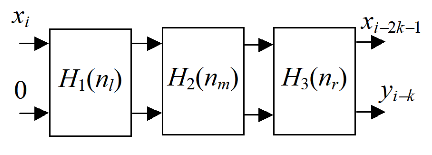
The FIR filter coefficient set is named as an impulse response H(n). It is proposed to implement the FIR filter from three units, which calculate the convolution to the left H 1 (n l ), middle H 2 (n m ), and right H 3 (n r ) subsets of the coefficients, n = n l + n m + n r. The respective SDF is shown in Fig.2.

Figure 2. Modified SDF
In the most of cases, the bit width of the coefficients H 1 (n l ), and H 3 (n r ) is much less, than the bit width of the coefficients H 2 (n m ). Therefore, it is favorably to implement the filter part, marked in Fig. 2 as H 2 (n m ), using the DSP48 blocks, and others parts using CCMs.In the last situation, the filter stage can be implemented as the small tree of adders with the small bit width. Such a tree can have both high throughput and small hardware volume.
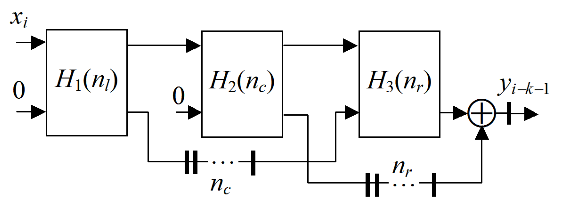
Due to this filter schema, the third filter unit must have the increased adder bit width to preserve the low level of the truncation errors. This can decrease the filter performance dramatically, because the long adder, based on LUTs, is much slower than the respective adder in the DSP48 block. To minimize this disadvantage, the improved SDF is proposed, which is illustrated by Fig.3.

Figure 3. Improved SDF
The proposed filter contains two parts H 1 (n l ), and H 3 (n r ) with the equal bit width, which is much less than the bit width of the DSP48 unit. The filter result is formed in the separate adder with the increased bit width. As a result, the designed FIR filter contains n m DSP48 blocks, which can be much less than the filter length n.
Experimental results. The design of FIR filters of the order of n = 35 for the input, output data, and coefficient bit width 16 was considered. The CCMs were built using the canonical signed digit coefficient representation [2–4], and the adder tree. The FIR filter design experience shows that about a half of the 16-bit filter coefficients can be represented in the canonical signed digit form using only four nonzero digits. For example, the filter stage, which performs the multiplication of x to 0.000000101101110 2 and addition of the sum of products p i from the previous filter stage, looks like the following:
p i+1 = p i + 2 −6 x −2 −8 x −2 −11 x −2 −14 x.
The modern FPGAs, which have the six input LUTs, support the design of the high-speed three input adders. So, such CCM with the addition of the sum of products is implemented in the two staged pipelined network of LUTs providing the maximum clock frequency. Under these conditions, the first and third filter units (see Fig. 2, 3) have both minimized hardware volume and high throughput.
The DFGs in Fig 1-3 were described by the VHDL language. Then, the filter projects were synthesized for the Xilinx Spartan-6 FPGA. The results of the synthesis for some low pass filter of the 33-rd order are shown in Table 1. To estimate the whole hardware volume Q, it was considered, that an 18-bit multiplier in the FPGA requires 200 equivalent LUTs for its implementation.
The Table 1 analysis shows that the filter structure based on DSP48 blocks, provides the maximum sampling clock frequency f C at the cost of the hardware volume. The second combined structure gives lower value f C, but it provides much less hardware volume and the better ratio of throughput to hardware volume f C /Q.
Table 1. Parameters of the FIR filters implemented in Xilinx Spartan-6 FPGA
| Structure | LUTs | Registers | DSP48 | Q | f C , MHz | f C/Q |
| Systolic | 0 | 0 | 33 | 33 | 390 | 11.8 |
| Modified | 772 | 1538 | 17 | 20.9 | 146 | 7.0 |
| Improved | 914 | 1639 | 17 | 21.6 | 267 | 12.4 |
Conclusion. A method of the systolic type FIR filter design for FPGA is proposed, which utilizes both built-in multipliers and application specific constant coefficient multipliers.The method provides both the increased filter length and minimized hardware volume providing the high throughput. The derived filter structure has approximately in two times fewer hardware multipliers than the usual filter generated by the tool like Xilinx Coregen.The resulting filter is represented by the VHDL program and therefore, it can be effectively implemented in FPGA of any type and manufacturer.
References.
- “Spartan-6 FPGA DSP48A1 Slice User Guide”. UG389, v1.2, Xilinx Inc. May 29, 2014. -46 p.
- U. Meyer-Baese, “Digital Signal Processing with Field Programmable Gate Arrays”. //Springer, 4-th Ed. 2014, 930 p.
- A. Sergyienko, V. Vasylienko, O. Maslennikow, “FIR filter soft core generator” // Prace IV Konferencji Krajowej „Reprogramowalne uklady cyfrowe”, RUC’2001. -Szczecin, Poland. 2001. pp. 167-172.
- M. Kumm, “Multiple Constant Multiplication Optimizations for Field Programmable Gate Arrays”. //Springer, 2016. 206 p.
