Configurable Microcontroller Array
Represented in PARELEC’02
O.Maslennikov,
Polytechnica Koszalinska, Poland,Email: oleg@moskit.ie.tu.koszalin.pl
Ju.Shevtshenko, A.Sergyienko,
National Technical University of Ukraine,Email: aser@comsys.kpi.ua
Introduction.
In the last decade the density of the field programmable gate arrays (FPGAs), their clock frequency, and routing capabilities are increased dramatically. These FPGA features provide their very high throughput when implementing the algorithms in the hardware. At present, the configurable computer architecture based on FPGAs is of great interest due to its flexibility and high throughput in a wide set of applications [1]. But using of such computers at the field of computing intensive applications is limited now because of the labor consumable process of mapping the algorithms into FPGA. The author’s experience in the development of the configurable parallel system for the QR – decomposition has proved this thesis [2].
One of the way to solve the problem of the configurable processor programming is the intellectual property (IP) core reuse. The another way is programming the parallel system of processing units (PUs), which is configured in FPGA.
In the representation the PU array is proposed which is configured in FPGA. Each PU is implemented as the IP core with the architecture of the well-known microcontroller i8051.
PU structure.
The standard i8051 microcontroller is characterized by the complex instruction set, among them bit handling instructions are very effective ones in many applications. But the original microcontroller has long instruction cycle (12 and 24 clock cycles) and comparatively large hardware volume. Besides, the data addressing space is limited and is unsufficient for many applications.
An IP core generator was developed, which generates the 8051 microcontroller soft core. This core is characterized by small instruction cycle and minimized hardware volume. The average instruction cycle is equal to 3 clock cycles, and the call, jump -type instructions are not succeed 4 clock cycles. The core is described by VHDL, and runs in Xilinx Virtex devices at the clock frequency of 60 MHz and higher.
The core hardware volume is exchanged in the range of 500 Ц 1100 configurable logic block (CLB) slices depending on the core functionality. In most of applications of the microcontroller array the core hardware occupies from 550 to 800 CLB slices, not taking into account block RAMs with PU program and data. The inner registered RAM has the volume 256 bytes. The program and data RAM can occupy 2 – 8 kbytes of synchronous block RAMs depending on FPGA device and program complexity. Besides, the core structure provides the direct access to the large and slow outer data memory. This core structure is described in [3]. For comparison, the analogous IP core DR8051 occupies 1045 CLB slices and runs at 56 MHz [4].
Processor array structure and its programming.
The processor array structure consists of n PUs and the global data RAM which are connected together through the common data and address bus (n=4,Е,100 ). It is shown on the figure 1. Processors are connected to the ring by local busses. The separate hardware arbiter controls the access consistency to the data RAM, which can be as large as 16 Mbytes.
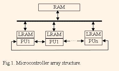
The user can program not only this ring structure but any array structure which is well fitted for the algorithm implementation. Additional hardware modules can be attached as well. The system is connected to PC through the PCI interface, and serves as the hardware accelerator.
This system is intended for the implementation of applications, which are characterized by the large volume of logic and bit calculations, and capability to be decomposed into a set of independent tasks. Such applications are morphological image processing, complex decision searching, genetic algorithms, etc. These applications are control intensive and are hard to be fully implemented in the hardware data path.
The microcontroller system configuring process has the following three stages. On the first stage the user microcontroller programs are analysed. By this process the unused instruction codes and the data addresses are fixed. For this stage implementation the Hexanalyser program was developed. This program disassembles the PU program codes, collects the command and address location statistics, and makes file of the PU VHDL model generic constants and file of the program ROM dates.
On the second stage the PU cores are generated, in which the unused units and logic cells are taken off automatically by the synthesizer like the Synopsys compiler. Each node program is mapped into the separate PU core. If the resulting architecture is the SPMD Ц architecture, then the only one PU core is generated. When the application needs the intensive calculation of some special functions, for example, long word operations, then the proper functional unit can be attached to the PU core as the special function registers.
On the third stage all the PU core netlists, or copies of a single PU core netlist are attached to the microcontroller array netlist, and the whole project is translated into the configuration file of the target FPGA device.
Experimental results.
The Hough transform and median, erosion, dilation filtering algorithms were selected as the applications of the configurable microcontroller array. The Hough transform consists in calculating the statistic of neighboring pixel distribution in the binary images to select straight lines in this image. The main loop of the algorithm implements the accumulator for each possible straight line pixel, which accumulates the number of pixels, which satisfy the line equation with the given slope. The resulting image is formed by pixels which accumulators exceed some threshold.
This algorithm is both computing and control intensive. In [5] the programmable processor array Systola was proposed to solve this algorithm, which consists of 1024 PUs, and is implemented in 16 ASICs. This array can be considered as a huge VLIW processor with the rigid architecture, and its programming is rather complex.
Two structures of the configurable microcontroller array were probed for implementation of the Hough transform algorithm. The first structure has 4 PUs, which are configured in the Xilinx XCV300 device, and the outer 8 Mbyte common data memory. One PU occupies 680 CLB slices. The structure is implemented in the VCC Inc. VCC-300 board. The average speed of this processor array is equal to 80 million instructions per second at 60 MHz clock frequency. The second structure has 12 PUs which are configured in the Xilinx XCV800 device of the Aldec Inc. HES board which is attached to the PCI interface. The algorithm is planned to be implemented in the HES board based on the XCV2000E device. The high-end XC2V8000 device can contain up to 70 PUs with the common peak speed, which is equal to 3000 million instructions per second at the 120 MHz clock frequency.
The algorithm implementation periods are given in the table 1 for different array structures. Here the scaled performance of the Systola array is given for the comparison. The processed binary image dimensions are 256 to 256 pixels. The pixel accumulators are 8 bit wide. The image was tiled to n interleaved stripes, which are distributed among PUs. Therefore the overheads to the data movings are negligible comparing to the calculations.
The derived figures show that the configurable microcontroller array capabilities can compete with ones of the application specific processor array.
The median, erosion and dilation filters were programmed in the configured microcontroller array as well. The subframe dimensions are 3*3 pixels, the processed image dimensions are 256*256 pixels. The derived speed characteristics are shown in the table 1.
TABLE 1. Time of Algorithm Implementation for Different Array Structures
| Structure | Clock frequency, MHz |
Time of algorithm implementation, s. |
|
| Hough transform | Median filtering | ||
| 1 standard i8051 | 24 | 810 | 21.6 |
| 4 PUs in XCV300-4 | 60 | 11.3 | 0.350 |
| 12 PUs in XCV800-4 | 60 | 3.77 | 0.120 |
| 24 PUs in XCV2000E-6 | 80 | 1.41 | 0.047 |
| 1024 PUs of Systola [3] | – | 0.062 | – |
Conclusions.
The proposed configurable microcontroller array is a good example of the configurable computing. It shows an effective way to speedup the implementation of both computing and control intensive algorithms. The proposed technique of mapping the program into configurable hardware showed the 1.5- 2 – fold hardware minimization. The use of well-known i8051 PU architecture simplifies the application programming. The designed microcontroller PU core has in 6 times higher instruction implementation speed, and in more than 2.5 times clock frequency than the original microcontroller.
In the last time the processor arrays with configurable interconnections start to propagate [7],[8]. Many tenths of RISC PUs on such a chip give the huge throughput. The proposed configurable microcontroller array can compete with these processor arrays in the case when the PU architecture has to be flexible one. It is very useful in such applications, where logic intensive calculations, or high speed byte handling computations are of demand. For example, such applications are homomorphic image processing, pattern recognition, genetic algorithms, neural nets, etc.
References.
[1] J. Villasenor, B. Hutchings, “The flexibility of configurable computing,” IEEE Signal Processing Magazine , vol. 15, pp.67-84, May 1998.
[2] A. Sergyienko, O. Maslennikov, “Implementation of Givens QR Decomposition in FPGA,” Lecture Notes in Computer Science, Springer, vol.2328, pp.453-459, 2002.
[3] V.Lepekha, A.M.Sergyienko, J.Kaniewski, “VHDL-Model of Ultrafast Microcontroller 8051,” Proc. 3-d Region. Conf. “Reprogramowalne Uklady Cyfrowe, RUC’2000”, Szczecin, Poland, pp.35-41, 2000.
[4] “DR8051 8-bit RISC microcontroller”. Data sheet. Available at www.dcd.com.pl/.
[5] B.Schmidt, M.Schimmler, H. Schroeder, “Morphological Hough Transform on the Instruction Systolic Array,” Proc. Euro-Par’97. pp.798-806, 1997.
[6] P.M.Embree and D.Danieli, “C++ Algorithms for Digital Signal Processing,” Prentice Hall, 579p. 1999.
[7] A. Calardo, “Comms warm a bit to reconfigurable processor,” EE Times, March, 30, 2001.
[8] P. Clarce. “Beefly parallel processor packs 128 cores,” EE Times. Sept., 10, 2001.