Implementation of IIR Digital Filters in FPGA
Represented in RUC’99, Szczecin, Poland
Anatoli Sergyienko*, Volodymir Lepekha*,
* National Technical University of Ukraine “KPI”, Kiev, Ukraine, email: aser@comsys.kpi.ua
Juri Kanevski**
** Technical University of Koszalin, email: kaniewsk@lew.tu.koszalin.pl
1. Introduction
Infinite impulse responce (IIR) filters are widely used in digital signal processing systems due to the following causes. IIR filters are rigorously analogous to well known and widely used ahalog filters. Finite impulse responce filters (FIR) have computatoinal complexity several times as much as IIR filters have.
In most cases IIR fiters are implemented by signal processors and ASICs, which architecture is adapted to filtering algorithms. For a long time IIR filters represent applications of FPGAs in the digital signal processing [1]. Implemetation IIR filters in FPGA has a set of advantages. Because of full adaptation of implemented in FPGA structure to the filtering algorithm, high throughput, hardware utilization effectiveness, any rate of calculating precision is achieved. In many special applications, like high speed communications, FPGA is the only solution for IIR filter implementation.
In the representation data flow graphs (DFG) for IIR filtering algorithm, its optimization, and mapping into the structure are considered taking into account structure forming properties of modern FPGAs.
2. IIR filtering algorithms and their representation by DFG
The approach to IIR filter syntheesis which is based on analog prototype transformation is commonly used. The differential equations which describe the prototype are changed to the difference ones, and Laplase transform is changed to Z-transform.
IIR filtering consists in solving the difference equation in the form:
yi = a0xi+a1xi-1+…+amxi-m+b1yi-1+b2yi-2+…+bnyi-n, i = 1, 2,…, m≤n
which represent the IIR filter of n-th order, computing the input dates xi into output dates yi. The folloving z-transform of the impulse responce corresponds to the difference equation.
H(Z) = (a0+a12-1+…+amz-m)/(1-b1z-1-b22-2-…-bnz-n) (1)
This Z-transform is equal to the frequency responce by z = exp(jω) and comparing to the IIR filter responce contains not only zeroes but also poles. IIR filter of n-th order can be represented by parallel or sequential connection of small order filters. Sequential connection of second order sections is widely used due to more small level of truncation error noise and computational stability.
Z-transform (1) is transformed to a data flow graph (DFG). By this process operator nodes represent operations of addition and multiplication, a chain of k delay nodes represents operator z-k, edges represent data flows. Besides calculations in numerator correspond to forward data flow chains, and calculations in denominator correspond to feedback ones. For example, Z-trans-form H(Z) which corresponds to the equation is transformed to the DFG which is represented by the fig. 1.
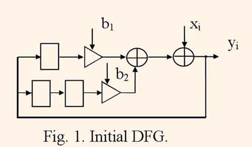
Here circle, triangle, and rectangle represent addition, multiplication to the coefficient, delay to one clock period.
An IIR filter structure which calculates with the period of τ = 1 clock cycle is derived by exchanging nodes of addition, multiplication and delay to multiply unit, adder, and register, respectively. This is so called identity mapping structure.
The minimum clock cycle period tc which defines the filter throughput equals to the maximum route length between neigboring delay nodes. For DFG represented by fig. 1, tc= tm+2ta, where tm and ta are equal to multiplication delay and addition delay, respectively.
Usually identity mapping structure has maximum throughput at the expence of high hardware cost. Practically, the filtering with a given calculation period τ > 1 which is derived from the quantization frequency of the computed signal fq = 1/(τ tc) by minimum hardware cost condition is necessary. Therefore, by the synthesis of the practically used IIR filter structure the more complex mapping than the identity one is usually used.
3. Transformations of DFG
Before the mapping of the algorithm and its DFG into the filter structure a set of optimization transforms, such as retiming, unrolling, look-ahead computation and pipelening is performed [2].
Retiming consists in transposition and moving delay nodes in DFG by the condition that the delay number in each cycle remains the same. Figure 2 illustrates one of the possible variants of retiming the DFG, which is represented by the fig.1.
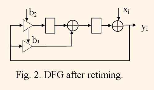
In derived DFG the delay node number is decreased from three to two, i.e. retiming helps to minimize the register number in the structure. Also the clock cycle period tc can be minimized in some limits by the retiming.
Usually DFG represents the i-th iteration of computing the given filtering algorithm. When DFG represents J neighboring iterations of the same algorithm computing, then such DFG is called unrolled by factor J, and the procedure of transformation DFG into unrolled one is called DFG unrolling [2]. Figure 3 illustrates DFG after unrolling DFG, which is represented by the fig.1, with factor J=2.
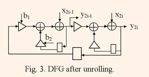
As a rule, mapping unrolled DFG gives more efficient structures, than mapping initial DFG because of increased scope for the operator scheduling [2].
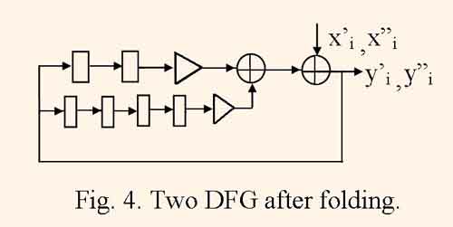
When DFG is folded, equal operator nodes, which are calculated in shared resources, are joined together, proper switch nodes are connected to inputs and outputs of derived operator nodes, parallel braches are substituted to one branch with all of delay nodes from substituted branches. In some cases the folding transformation is the inverse one to unrolling. If initial DFG consists of J equal unbundled DFGs then the resulting DFG is equal to one of DFGs with J times increased number of delay nodes. The mapping of such folded graph gives the structure which implements J parallel filter channels with period of τ = J clock cycles. Figure 4 illustrates DFG after folding two DFGs, which are represented by the fig.1, and figure 5 illustrates the same DFG after retiming.
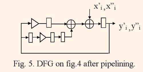
One can to see that for the DFG, which is represented by the fig.5, the minimum clock cycle period is equal to tc = max (tm , 2ta), and is less than the one for initial DFG.
The look-ahead computation means the algebraic transformation of the filtering algorithm, which minimizes resulting clock cycle period [2]. But often the look-ahead computation causes a large increase of computational complexity. For example, joining calculations of two iterations of the equation (2) gives the following equation: yi=xi+bixi-1+(b12+b2)yi-2=b1b2yi-3, which is represented by DFG illustrated by fig. 6.
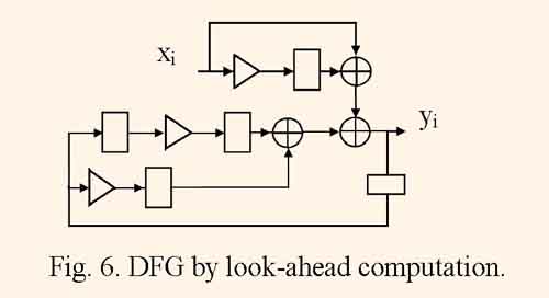
For derived DFG the minimum clock cycle period is equal to tc = tm+ 2ta, and is less than the one for initial DFG.
By the pipelining a set of delay nodes is added to DFG and the retiming is perforned to achieve the minimum clock cycle period tc by the condition that the initial algorithm remains the same. When the multiplication operator is decomposed to some stages the pipelining yields the extremally minimum clock cycle period. Many references deal with pipelining transformations, for example, [3,4]. The pipelined structures of FIR filters are very popular but the pipelining of IIR filter structures has limited opportunities. This fact is explained by the rule that it is impossible to enter the delay nodes into feedback chains without exchanging the initial algorithm. Therefore, before pipelining one has to apply look-ahead computation or DFG folding which produce additional delay nodes into feedback chains. Therefore, the limited number of delay nodes in feedback chains [4].
4. Mapping DFG into IIR filter structures
The structural models of ASICs for the digital signal processing can be divided into wide groups: structures derived by identity mapping, microprogrammable structures and application specific pipelines [5].
Structures derived by identity mapping have the large throughput. But in case of full bit parallel calculations the high hardware costs of such structures often do not permit their implementation in FPGAs. Therefore often the identity mapping is performed to synthesize the structure with bit serial calculations, which provides small hardware cost and pipelined computations. But in this case the quantization frequency must be equal to fq = 1/(ntc) , where n is the word length.
Many CAD tools design microprogramable IIR filter structures for ASICs [3,6]. Microprogrammable structural model consists of a set of resources like multily units, adders, registered storage units that are connected together by a set of shared busses. The DFG mapping consists in implementation of operator scheduling and allocation. The resulting set of resources and microprogram are formed using results of these two stages of the structure synthesis. After several mapping iterations a set of optimized structural solutions is derived which are differentiated in harware cost, and computation period τ. The structure optimization consists only in manipulation with the amount of resources. And therefore the microprogrammed structural model is rather limited and can not satisfy structural properties of FPGA such as computation pipelining, minimizing multiplexor inputs, etc.
The aplication specific pipeline both reflects most of particularities of digital signal processing, and mostly satisfies structural properties of FPGA. Pipelined structures which are implemented in FPGA can provide the achievement of its clock frequency limits.
Othen the DFG mapping into pipelined structure is implemented in such a way. The structure graph is derived by DFG folding, then an operator schedule is searched [3]. Figure 7 illustrates the IIR filter structure which is derived by folding DFG represented by fig. 1.
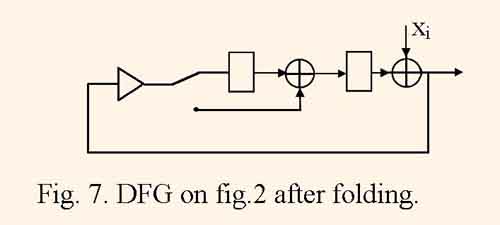
This structure computes the filtering with the quantization frequency fq = 1/(2(tm+2ta)) which is half as many as clock frequency is, and contains only one multiply unit.
The number of different folded DFG is increased exponentially by increasing of the algorithm complexity. Besides, DFG must be optimized by retiming and pipelining. Theretore the searching of optimized folded DFG is often too tedious. Several methods of pipelined structure design were developed which contain a set of heuristics to minimize the structure synthesis complexity [3, 6].
In the represetation [7] a method for mapping DFG into pipelined structure is proposed. The method is based on the representing DFG in multidimensional space with time, resource number, operation type coordinates and its mapping into subspaces of structures and events. Searching for the optimized structure is implemented by the linear algebra and linear programming methods. The operator sheduling and allocation are performed implicitely and simultaneonsly by the direct searching and therefore the optimization process has decreased complexity. Derived structures are operating in pipelined regime prowiding hiqh hardware utilization effectiveness and minimized clock cycle period. These structures do not need structural verification because they are synthesized by formal rules using injective and monotone mapping function.
Figure 8 illustrates the filter structure which is derived in [7] from the DFG on the fig.1.
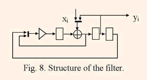
Here bold lines represent multiplexers. This structure computes the signal with the quantization frequeney fq = 1/(2tm) which is rather higher than the same frequency of the structure in the fig. 7 which has approximately equal harware cost. This fact also means that this structure can have equal throughput as the structure derived by identity mapping of DFG on fig. 1 or 2 has by the condition tm = 2ta, and have one adder and one multiply unit fewer.
By the given computation period τ ≥ 2 this method can optimize DFG by its retiming and pipelining simultaneonsly with its mapping into the structure. As a result, the 2, 3 and more staged pipelined multiply units can be synhesized in the structure of the IIR filter and therefore the clock frequency of the target FPGA chip can achieve its limitations.
5. Parametrized IIR filter structure library
Using the new mapping method IIR filter structure library is developed. The library contains a set of parametrized IIR filter structures and is intended to computer aided design of digital signal processing system on the base of FPGAs. The library consists of structural models of filters described by VHDL language in synthesable style. The structure parameters are: filter order nf = 2,3,…,10; computation period τ = 5,6,…, 20. The second order filter is calculated according to DFG which is schown on the fig. 9.
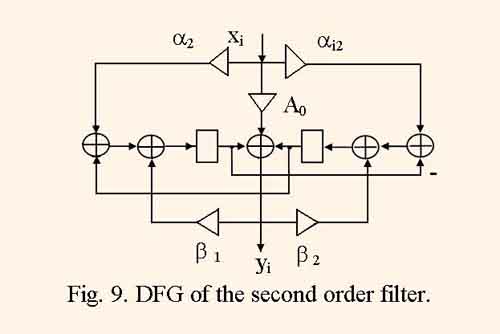
The Z-transform of this filter is equal to
A0+A1Z -1+A2Z -2
H(z)=—————————— ,
1+B1Z -1+B2Z -2
besides, α1 = (A0+A1-A2 ) / 2; α2 =( A1+A2-A0) / 2; β1 = (B2-B1-1) / 2; β2 = (1-B1-B2 ) / 2.
Such algorithm of IIR filter calculation, called wave propagation filter, guarantee computations without parasitic oscillations, and minimized truncation error noise, which are considered to be the serious disadvantage of usual IIR filters [8]. Besides, all of coefficients are less than one by its magnitude, and the truncation error noise is minimized.
The DFG of this algorithm was mapped into the IIR filter structure which is illustrated by the fig.10 using the method described above.
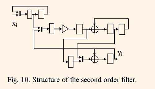
The advantages of this structure are small hardware cost and pipelined computations which are proved below.
The analyse of DFG and resulting strucrture represented by fig. 9,10, shows that without pipelining and by computation period τ = 1 and identity mapping the minimum clock cycle period is equal to tc1 = tm+3ta , and the hardware cost consumes five multiply units and six adders. And in synthesized structure of the filter with τ = 5 due to the its full pipelining, the minimum clock period is equal to tc2 = tx + max(ta , tm /2) , where ta is adder delay, tm is full multiply unit delay, and tx is multiplexor delay, and the hardware cost consumes one multiply unit with two staged pipeline and two adders. Therefore, the pipelined filter structure throughput decreases by a factor of τtc2/ tc1≈ 1.2,…,1.5, and hardware cost decreases by a factor of ≈ 4 . As a result, the throughput – cost rate increases approximately in three times.
In the filter structures the addition is performed for one clock period, the multiplication lasts two or three clock periods. But the two or three staged pipelined parallel multiplier derives products every clock cycle. Usually the coefficients are known constants, therefore the multiply operation is performed using tables of coefficients multiplied by a set of natural numbers, which substantially minimizes the hardware cost.
6. Conclusion.
Implemetation IIR filters in FPGA has a set of advantages, like full adaptation of implemented in FPGA structure to the filtering algorithm, high throughput, hardware utilization effectiveness, any rate of calculating precision. The DFG of the filtering algorithm is mapped into the structure of the filter. But due to the feedback chains in IIR algorithms such methods of algorithm optimization like retiming and pipelining give limited results. But using look-ahead computations something increases the algorithm parallelism at a sacrifice in the hardware cost increase. In the case when the clock frequency is τ =2,3,… times as much as the quantization frequency of the digital signal, there are a wide opportunity to enlarge pipelining of IIR filter calculations, and therefore to derive filter structures which support maximum hardware utilization and high clock frequency when implementing in FPGA.
Authors propose the method for mapping DFG into the IIR filter structure, which helps to design filters with high characteristics. This method shows good results by the development of the library of IIR filter structures. The library contains a set of parametrized IIR filter structures and is intended to computer aided design of digital signal processing systems on the base of FPGAs. The library consists of structural models of filters described by VHDL language in synthesable style. The structure parameters are filter order and computation period τ.
References
1. J. Isoaho, J. Pasawn, O. Vaino, H. Terhunen. DSP System Integration and Prototyping With FPGAs. J. VLSI Signal Processing, 1993, № 6, p. 155-172.
2. K.K. Parhi. Algorithm transformation techniques for concurrent processors. Proc. IEEE. 1989, V. 77, № 12, p. 1879-1895.
3. K.K. Parhi. C.Y. Wang, A. D. Brown. Synthesis of Control Cirсuits in Folded Pipelined DSP Architectures.
4. Renfors, Y. Nenvo. The maximum sampling rate of digital filters under hardware Speed constraints. IEEE Trans. Circuits Syst. 1981. V.CAS-28, N 3, p. 196-202.
5. H. Mann, F. Kathor, G. Hossens J. Vanhof. Methods of arichitectural synthesis for mapping signal processing algorithms into ASICs. Proc. IEEE. 1990, V. 78, № 2, p. 319-335.
6. The Systhesis Approach to Digital System Design / Ed.: P. Michel, U. Lauther, P. Duzy. Kluwer Academic Pub. 1992.
7. A. Sergyienko, A. Guzinski, Ju. Kanevski. A method for mapping unimodular loops into application specific parallel architectures. Proc. 2-nd Int. Conf. on Parallel Procesing and Applied mathematics. PPAM’97. Zacopane, Poland, Sept. 2-5, 1997, p. 362-371.
8. A. Fettweis, K. Meer Koetter. Suppression of parasitic oscillations in wave digital filters. IEEE Trans. Circuits Syst. 1975. V.CAS-22, N 3, p. 239-246.