Methods of Mapping DSP Algorithms into FPGA
Oleg Maslennikow
Technical University of Koszalin, Poland, Email: oleg@moskit.ie.tu.koszalin.pl
Anatolij Sergiyenko
National Technical University of Ukraine “KPI”, Kiev, Ukraine, Email: aser@comsys.kpi.ua
Abstract
A method of mapping DSP algorithms into FPGA is considered. Algorithms are represented by synchronous data flow graphs, and are mapped into pipelined data path. The Method consists in placing the algorithm graph in the multidimensional index space and mapping it into structure and event subspaces. The limitations to the mapping process minimizes both clock time and hardware volume including multiplexor inputs.
1. Introduction
Modern field programmable gate arrays (FPGAs) have the volume of millions of equivalent gates and hundreds of hardware multipliers. The FPGA clock frequency achieves hundreds of megahertz. Therefore they are considered as advanced chips for high throughput digital signal processing (DSP).
By the behavioral or high level synthesis of computing systems the DSP algorithm is usually represented by the synchronous data flow graph (SDFG). In SDFG the nodes, which are named as actors, represent the algorithm operators. Edges represent variable movings between actors with the delay to a given cycle number. During a single cycle each actor generates and accepts a variable (token) set, which volume is stable in each cycle [1],[2].
The Synthesis of computing system usually has three general tasks: resurce allocation, operator (or actor) scheduling, and binding resources with operators. These tasks consist of subtasks like variable moving scheduling, variable to register or bus assignment, memory allocation, etc. The different synthesis methods are distinguished due to the order and way of such subtask implementation. The operator scheduling is the responsible and complex task.
DSP algorithms have both cyclic and acyclic SDFGs. In general, the subgraphs of the cyclic SDFG have different computing periods. The multirate DSP system is an example of such SDFG. Therefore the SDFG sheduling is a complex task. Very popular approach consists in the search for the shedule of an algorithm period, considering the acyclic part of SDFG. Here the algorithms of list scheduling, force directed scheduling, graph colouring, left edge scheduling are very popular. But these methods cause the bad load balance of processing units (PUs) at the beginning and the end of the cycle. To consider the cyclic nature of SDFG the conflict graph or interval graph are analysed additionally [2],[3].
The resulting computing system effectiveness depends on all synthesis task implementation. But they are usually implemented separately. The subtasks have the local targets, which are often in contradiction to another subtask targets. Therefore most of synthesis methods do not provide the effective structure solutions.
Recently such programming tools like AccelDSP or System Generator are wide-spreaded, which help to generate the FPGA configuration of the DSP computing system. Here the initial algorithm is represented by SDFG using Matlab Simulink package [4]. But these tools are effective ones only for аcyclic SDFG, for example, FIR-filters, or for actors which represent the complex library components.
In [5],[6] methods for mapping SDFG into parallel computing structures are proposed. They are based on placing the graph in the multidimensional index space and mapping them in subspace of structures and subspace of events. Methods of structural design of digital filters described in [7],[8] use this approach as well. This approach provides simultaneous fulfillment of the synthesis tasks and therefore it optimizes the structure of computing system much better. In the representation this approach is described in the application of mapping DSP algorithms into FPGAs.
2. Mapping SDFG into subspaces of structures and events
The initial dates for computing system design are DSP algorithm, represented by SDFG and cost functions. SDFG with a single discretization frequency is considered. Multirate SDFG is transformed into equivalent single rate SDFG. The computing system structure consists of a set of processing units (PUs), connected to each other according to the structure graph. PU consists of ALU of given type (multiplier, adder, etc.) with the result register (or FIFO buffer ) on its output and with the multiplexers on its inputs. PU calculates the operation not more than for a single clock cycle. If PU has not a register then the operation is considered to be calculated without delay. Such simple PUs can be naturally implemented in the FPGA hardware including special DSP hardware in modern FPGAs like DSP48 units in Xilinx Virtex4 devices.
The cost functions are algorithm period interval QT = Ltc and hardware cost:
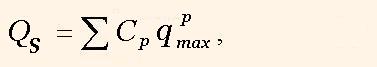
where L – period, clock cycles, tc – clock cycle length, Сp – hardware cost of PU of p-th type.
Due to the method SDFG is represented in the three dimensional index space as the algorithm configuration KG = (K, D, A), where K – is the matrix of vectors-nodes Ki , representing algorithm operators, D is the matrix of vectors-edges, representing variable movings between operators, A is the incident matrix of SDFG. The coordinates of the node Ki = < ki , si , ti > are equal to the operator type (for example, k = 1 is multiplication), PU number si , in which the operator is implemented, and clock cycle ti , when the operator result is stored in the register.
Equivalent structural solutions are represented by equivalent algorithm configurations, which of them differ in its matrices К and D. The matrix К codes some correct solution, and the matrix D can be derived from the equation D = КА . The optimum structural solution finding consists in the search of the маtrix К , which minimizes the given cost criteria. If the genetic optimization approach is used then the matrix К serves as the genome of the population representative. The following relations and definitions help to find the effective solutions.
The algorithm configuration is correct if there are none equal vectors in the matrix К, i.e.
∀ Ki , Kj (Ki ≠ Kj , i≠ j ) .
The operator schedule is correct if the operators, that are mapped in a single PU, are implemented in different clock cycles, i.e.
∀ Ki , Kj (ki = kj , si = sj ) ==> ti ≠ tj mod L.
Here the modulo operation considers the cyclic nature of SDFG implementation. The equal operators are mapped in the PUs of the same type:
Ki , Kj ∈ Kp,q (ki = kj = p , si = sj = q ), | Kp,q | ≤ L,
where Kp,q is a set of nodes of p-th type, that are mapped into q-th PU.
If SDFG has a cyclic route i then the sum of vectors-edges Dj , belonging to this route, has to be equal to zero
∑ bi,j Dj = 0,
where bi,j is the not zeroed element of i-th row of the cyclomatic matrix of SDFG. Such cyclic routes are inherent to the IIR filters. And the back propagation, reversed vector-edge DВj = < 0,0, – kL> means the delay which is equal to k periods (iterations) of the algorithm. This vector is equivalent to the delay node Z–i in the signal graph of the DSP algorithm.
SDFG can be represented as the conjunction of the аcyclic subgraph, which implements the calculations of a single algorithm period, and a set of reversed edges DВj. In the multidimensional space these edges are directed in the reversed direction relatively to the time axis оt. They represent the interiteration delay to kL clock cycles.
Effective configuration is searched in two steps. On the first step SDFG nodes and edges are placed in the three dimensional space as sets of vectors Ki and Dj with respect to all conditions mentioned above. Then the PU number is minimized satisfying the condition | Kp,q| → L. This condition means that the number of nodes, that are mapped into a single PU, is directed to L.
On the second step the configuration balancing is implemented. For this purpose the acyclic subgraph of SDFG (i.e. it is without reversed edges DВj) is considered, and in each its edge the delay nodes are added. These nodes represent the delay or storing to a single clock cycle, or register. In the resulting balanced configuration all the vectors-edges except reversed vectors are equal to Dj = < aj , bj , 1 > or Dj = < aj , bj , 0 >. The nodes form columns, and the distance between neighboring columns is equal to one clock cycle.
The balanced configuration is optimized by mutual interchandes of nodes belonging to a single column. By this process the register number and the multiplexor number are minimized. The other methods like resynchronizing, left edge shedule are used sa well.
The computing system structure and the resulting schedule are derived by splitting the algorithm configuration KG to the structure configuration Ks and event configuration, that have the same incidence matrix А. The vectors of the structure configuration are equal to < ki , si >, i.e. to the type and number of PU, and the vectors of event configuration are equal to < ti >, i.e. to the clock cycle in which the mapped operator is implemented. In such a way the algorithm configuration is mapped into the structure subspace and into the event subspace.
3. Method for multiplexor minimization
Consider the method of multiplexor minimizаtion in pipelined computing system which is effective for FPGA projects. Very often SDFGs of DSP algorithms have a set of isomorphic subgraphs. For example, algorithms of complex IIR filters are the chains of the second order stages, FIR filter graphs have equal periodic parts. High speed recursive filter structures are designed composing identical all-pass subfilters [9]. To minimize the multiplexor number in such structures the following theorems are used.
Theorem 1. Consider the balanced algorithm configuration. Then the multiplexor input amount NМi of i-th PU node not succeeded the number of vectors Dі,j that are not equal to each other, and its arrows are incident to the nodes Ki,k , mapped in this PU.
The theorem proving is evident. Such vectors Dі,j represent the variables that are inputted in i-th PU through different multiplexor inputs. The words “not succeeded” means the occasion when the multiplexor has a single input and is not needed at all. In another situation the multiplexor input number is equal to the different vector-node number.
Theorem 2. Consider the balanced algorithm configuration KG which has up to L isomorphic subgraphs, or equivalent subconfigurations KGОі = (KОі , DОі ,AO ). Then the structure, which is the result of this configuration mapping with the period L, has the minimum multiplexor input number if and only if all the subconfigurations KGОі are mapped into a single structure subconfiguration KSО , and
∀ Ki,j ∈ KОі ( Ki,j = < Cj,k , Cj,l , ti,j > ) ; (1)
∀ Ki,j ∈ KОі (arrow of Di,l is incident to Ki,j ==> Di,l = < Ck , Cl , 1 > , Cl ≠ 0 ) (2)
This means that the structure subgraph is isomorphic to the proper algorithm subgraphs. Figure 1 illustrates mapping the algorithm configuration with the period L = 3 to the structure configuration. Bold line represent the multiplexor.
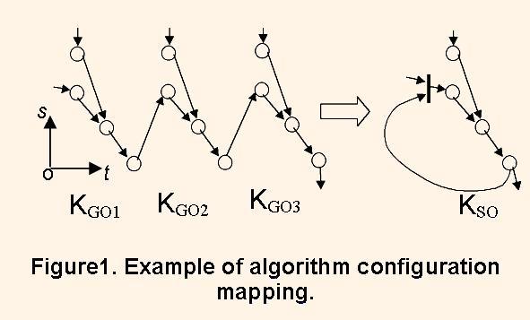
The theorem proving. When the conditions (1) and (2) are satisfied then the resulting PU with one input ALU has a single input, and with the two input ALU has two inputs respectively. This means that each PU of resulting subconfiguration has none multiplexor at all, not to consider the inputs of PU (see the Fg.1).
From the opposite side, consider the theorem conditions are satisfied. Let one or two nodes in the subconfigurations exchange their coordinates. Then two situations can be held on. In the first one the interchanged node will be mapped into additional PU node, which increases the hardware volume. Besides, the vector Di,l , which is outputted from this node, exchanges its coordinates. And in the resulting structure the additional multiplexor input occurs in which the data is outputted from the additional PU node.
In the second situation the node is mapped into another free PU node, or two nodes are mutually interchanged. Then the two input multiplexers have to be set on the inputs of this PU, or these PUs. As a result, the conditions (1),(2) are not satisfied by any exchanges in subconfigurations, which cause the increase of PU number or multiplexor input number.
4. Method for synthesis of digital filters with multiple delays
Usually digital filters are described by the transfer function H0(Z) which depends on the complex variable Z . This function represents the filtering algorithm with the period L = 1 precisely. And each multiplicand Z-k in the function represents the delay to k cycles, which can be implemented on the FIFO with k registers. If the register number in each delay FIFO is increased in n times then the filter with the function Hn(z) = H0(Zn) is derived. Such a filter, named the filter with multiple delays, has the following property. Its frequency characteristic is similar to the prototype filter characteristic but in the range of 0 to fs these characteristic repeats itself n times, where fs is the quantization frequency.
Besides, in Xilinx FPGAs the multiplied delays are inplemented in FIFO units of SRL16 – type, which occupy the same place as separate registers do. For the synthesis of filters in FPGA the following method is proposed.
On the first step of the method the algorithm is selected which SDFG has a set of isomorphic subgraphs. The subgraph edges can be loaded by delays which are equal to k . Consider the subgraph number is L . This figure provides the maximum hardware utilization but in general, it can have another value. The subgraph with k = 1 is represented by the algorithm subconfiguration named as period configuration. The border nodes in it are selected which are incident to the reversed edges. These border nodes are mapped into iteration inputs and outputs of the structure. The period configuration is optimized as it is mapped into the structure with the parameter L = 1 clock cycle, i.e. the structure with the maximum parallelism.
On the second step up to L subconfigurations and other nodes (if needed) are connected together according the algorithm graph. By this process the conditions of the theorem 2 are satisfied. If some filter stage uses delays to k cycles then (k – 1) L delay nodes are added to reversed edges of its subconfiguration.
On the third step the configuration is mapped into the structure with the period L. The resulting structure consists of the pipelined substructure which implements the period configuration, and multiplexers with delays to (k – 1) L clock cycles on its inputs.
The hardware volume of the resulting structure, not to account registers, is estimated by the formula:
θS = nA + 10nM + 0,57LnD ,
where nA and nM is the adder and multiplier number adders and multiplication units, which is equal to the number of nodes of additions and multiplications in the subgraph of SDFG; nD is the number of reversed edges, or delay lines in the filter stage.
The register number in the structure depends on the topology of the subgraph, on the delay distribution between reversed edges, and can be estimated as the number which is proportional to L. As a result, if the subgraph number is equal to L , then the structure has the minimum number of registers, adders and multipliers. This is proven by the fact that by this condition exactly L nodes of delay, addition, and multiplication are mapped into respective PU nodes, and all of them are fully loaded.
5. Filter synthesis example
Consider the example of the low pass filter structure synthesis using the methods described in [9]. The filter consists of four sequential stages with the delays multiplied by 1, 2, 4, and 8. First three stages have the transfer characteristics as the bireciprocal filter has. The last stage frequency characteristic forms the sharpness of whole filter. Each stage is implemented on the base of allpassfilter, and therefore it has stable, and well regulated characteristics. The transfer function of a single (first) stage is the following
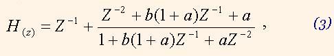
where b regulates the pass band cutoff frequency, a regulates the filter sharpness. This filter is effectively implemented using the two staged lattice wave digital filter structure which provides the minimum of multipliers [11].
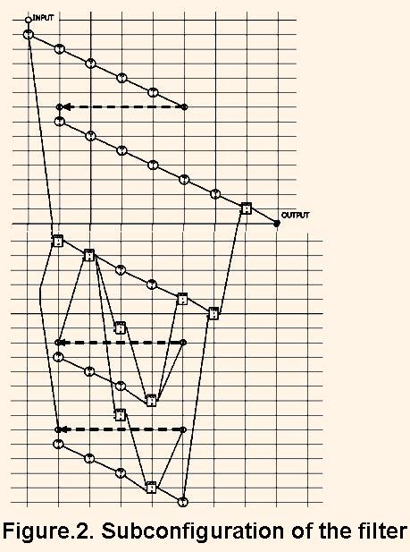
On the first step of the synthesis the balanced algorithm subconfiguration is formed which is shown on the Fig.2. On this figure the register nodes are signed by large circles, reverse edges are signed by the dotted arrow, and border nodes – by small circles. The time axis is horisontal and the space axis is vertical.
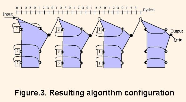
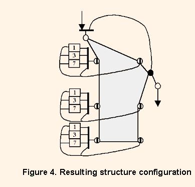
On the second step L = 4 subconfigurations are connected together. The resulting configuration is shown on the Fig. 3. And on the third step the filter structure is derived, and its FSM is synthesized. The derived structure configuration is illustrated by the Fig.4. In the figures the colored polygons represent the subconfiguration shown on the Fig.2.
The filter implementation consists in transformation its algorithm configuration into VHDL description and then in configuring it in FPGA.
When such a filter is designed by the usual method then its structure consists of four separate stages connected in chain. Each stage has 7 adders 2 multipliers and 3 registers for pipelining. Besides these stages have three registered delays, each of them has 1, 2, 4 and 8 registers, which can be implemented on SRL16 units. The resulting hardware volume is equal θSВ = 132. In the critical path of this structure 4 adder are set, i.e. the clock cycle period is equal to θТВ = 4ТS.
The synthesized structure has 2 multipliers, 7 adders, 26 registers and registered delays, and 7 four input multiplexers. As a result its hardware volume is equal to θS = 65,5. The critical path delay is equal to the delay of a single adder or multiplier, i.e. θ>Т = ТS, and the cycle period is equal to LТS = 4ТS . Comparing the derived figures, the proposed structure has twofold smaller hardware volume than the usual structure has, and has the same throughput.
6. Dynamically tuned Digital filter
In the representation the digital filter that is tuned dynamically (on the fly) is represented. This filter design is similar to the design example shown above. The main idea is that the stage coefficients, and the chain length can be exchanged during the filter operation considering the properties of the transfer function (3). Up to 8 stages are connected into chain. As a result, the bandpass edge frequency is tuned in the range of (0,015-0,4)fS . The suppression level is not less than 75-80 дб, and the filter sharpness is not less than 100 db per octave. The 12-bit length frequency code regulates the edge frequency.
The filter was implemented in Xilinx Virtex2-Pro FPGA device. Its hardware volume occupies 706 CLB slices and three multipliers. Due to the full pipelining the maximum clock frequency is equal to 190 MHz. As a result, the filter has small hardware volume, high characteristics, and can operate with the signals with the sampling frequencies up to 24 MHz. The filter structure and control is so complex that its design would not impossible without new method use.
References
[1] S. S. Bhattacharyya, R. Leupers, P.Marwedel, “Software Synthesis and Code Generation for Signal Processing Systems” IEEE Trans. on Circuits and Systems—II: Analog and Digital Signal Processing, 2000, V47, №9, pp.849-875.
[2] The Systhesis Approach to Digital System Design / Ed. P. Michel, U.Lauther, P.Duzy, Kluwer Academic Pub., 1992.
[3] Eles P., Kuchinski K., Zebo P., System Synthesis with VHDL, Kluwer Academic Pub., 1998.
[4] http://www.xilinx.com
[5] Ju.S.Kanevski, A.M.Sergienko, A. A. Guzinski, “Method for Mapping Unimodular Loops into Application Specific Parallel Structures”, Proc. of the 2-nd Intern. Conf. “Parallel Proc. and Appl. Math. PRAM’97” , Zakopane, Poland, 1997, pp. 362-371.
[6] A.Sergyienko, J.Kaniewski, O.Maslennikov, R.Wyrzykowski, “Mapping regular algorithms into processor arrays using software pipelining” Proceedings of the 1-st Int. Conf. on Parallel Computing in Electrical Engineering, Bialystok, Poland, 2-5 Sept., 1998. pp.197-200.
[7] Ju.S.Kanevski, L.M.Loginova and A.M.Sergienko, “Structured Design of Recursive Digital Filters” Engineering Simulation, OPA, Amsterdam B.V., 1996, Vol. 13, pp. 381-389.
[8] A.Sergyienko, J.Kaniewski, A. Arefjev, D.Kortshev. A Method for Mapping DSP Algorithms into Pentium MMX? Architecture. Proc 3-d Int. Conf. On Parallel Processing and Applied Mathematics, PPAM’99, Kazimierz Dolny, Poland, Sept. 14-17, 1999, pp.348-356
[9] H. Johansson , L. Wanhammar, “High Speed Recursive Filter Structures Composed of Identical All-Pass Subfilters for Interpolation, Decimation, and QMF Banks With Perfect Magnitude Reconstruction”, IEEE Trans. on Circuits and Systems – II Analog and Digital Signal Processing, 1999, V46, N1, Jan., pp.16-28.
[10] J. G.Chung, K.K.Parhi, “Pipelined wave digital filter design for narrow-band sharp-transition digital filters” Proc. IEEE Workshop VLSI Signal Processing, La Jolla, CA, 1994, pp. 501-510.
[11] A. Fettweis, “Wave digital filters: Theory and practice”, Proc. IEEE, 1986, V74, N2, Feb., pp.270-327.