VHDL – Model of Ultrafast Microcontroller 8051
Represented in RUC’2000, Sczecin, Poland
V.L.Lepekha, A.M.Sergyienko
National Technical University of Ukraine “KPI”, Kiev, Ukraine, Email: aser@comsys.kpi.ua
Ju.S.Kaniewski,
Technical University of Koszalin, Poland, Email: kaniewsk@lew.tu.koszalin.pl
Abstract
The VHDL model of the microcontroller 8051 is represented. This model can be considered as an advanced IP core, and is intended for configuration in Xilinx Virtex™ and Spartan II™ FPGA devices. The questions of reusability and throughput characteristics of microcontroller IP cores are highlighted. The question of microcontroller speed estimation is put forward. The approaches of the clock frequency maximizing of such cores are proposed. The described model has extremally high clock frequency and short average instruction period as well as minimized interrupt handling delay.
1.Introduction
The reusable modules draw the attention of designers who develop systems on the chip (SOC). These modules called IP cores can be easily adapted to concrete conditions and technology of the new system. Most importanly, the use of these cores schortens the time-to-market for new systems due to their reuse.
Microcontrollers represent a significant class of IP cores because the main customer properties of SOC mostly depend on their characteristics. The architecture I8051 is considered to be the industrial standard of microcontrollers. Therefore The microcontrollers which represent this architecture are very often embedded in SOC. At present more than thirteen corporations propose their 8051 IP cores to SOC. These cores are differentiated to the hardware description level as soft (register transfer level), firm (netlist), and hard (layout). The soft cores are most flexible and technology-independent. Such cores give the profit of design cycle shortening and of low single chip cost when they are configured in FPGA. But the configuration developers must do efforts to optimize hardware volume, speed and/or energy consumption of these cores in the system.
The VHDL model of 8051 microcontroller which is proposed in the representation is a soft one. Its high potential speed and reasonable hardware volume provide system differentiation features or minimizing power consumption when running the software at slower clock frequency, lighten designer’s optimization efforts.
2.Microcontroller model metrics
Reusability, speed, and hardware volume are the most important characteristics of microcontroller cores from the customer point of view.
The reusability is a most valuable property of embedded cores which guarantees its successful use. First of all the reusable project must exactly agree its specification. This means that the reusable core must have good documentation, fully commented HDL texts, robust scripts for synthesis, and implementation, effective verification tools.
The way is very important that a set of microcontroller modifications with different memory volume, peripheral device sets, interrupt sources, etc., is generated by easy set-ups. The technology independence supports the reusability, and means the possibility to configure the microcontroller core into FPGAs of several vendors [1]. The description of the model in VHDL has advantages not only to be reconfigurable and technology independent but also to do its modelling and synthesis on the simulators and compilers of several vendors. This fact also proves its good reusability.
Both maximum clock frequency and number of clock cycles in a single instruction period characterise the speed of the microcontroller. The high clock frequency supports more wide scope for the system use. It also demonstrates small critical paths in logical schemes that helps to control the project implementation.
The original I8051 microcontroller implements its instruction for 12, 24, or 48 clock cycles. Two decades ago such solution minimized the hardware, supported the integral cicruit technology with latshes, and provided the interface to slow peripheral devices. At present, when this microcontroller model is put into SOC with all of peripheral devices, the number of clock cycles in the instruction period is to be minimized. Such minimization can dramatically increase the microcontroller speed without increasing its clock frequency. Besides, the reusability requires the fully synchronous schemes, and a single clock signal is of demand. In these conditions minimized clock period gives possibility to lighten the mutual synchronization of several blocks on the chip.
Therefore, many vendors propose 8051 microcontroller models with the shortened instruction cycle. For instance the microcontroller model which is is implemented on the chip EZ_USB has the instruction cycle which is equal to CI = 4,…,16 clock cycles [2]. The microcontroller model Flip805x-CR has the instruction cycle CI = 1,…,7 [3]. Such instructon cycle minimization gives reserve of the system throughput or saving in energy consumption depending on the concrete technology.
There is a proglem of comparing the speed of such controllers because its different instructions have different cycles. For example, in notes [2] the speed of the microcontroller in EZ_USB chip is estimated as the average instruction period which is equal to the sum of periods of all instructions divided by its number. As a result, this microcontroller has decreasing of the average instruction cycle CIA comparing to one of the standard microcontroller CIAO , which is equal to CIAO/CIA = 2.5 times.
In real customer’s programs some instructions are executed quicker than another ones, and some instructions do not executed at all. Execution frequency and time period of some instructions substantially inferrs the speed of the system. Therefore, the arithmetic mean instruction cycle is very coarse and robustless for the speed comparing.
The average instruction cycle can be estimated more exactly as the number of instruction cycles of concrete program execution which is divided by the executed instruction number. But the microcontroler model is developed for uncertain application to satisfy demands of a large set of customers. And the standard package of benchmark programs for the microcontroller 8051 is still not adopted.
If all the instructions are divided to some number n instruction subsets according to the defined attribute then the more exact average instruction cycle can be estimated as:
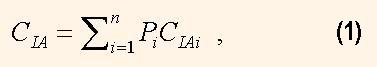
where PI is the execution probability of the instruction from the i-th subset, CIAi is the arithmetic mean instruction cycle in this subset. A set of 255 instructions of the I8051 microcontroller can be divided to n = 5 subsets: short move-type instructions, long move-type instructions, which are executed in I8051 for 12 and 24 clock cycles, respectively, bit handling instructions, arithmetic and logic instructions, and control instructions like jumps, calls, returns.
The instruction execution probability PI depends on the nature of the application. The Table 1 shows the values PI and CIAi for control and DSP applications. These values were derived from real programs for slot-mashine controllers, and harmonic measurers.
| Instruction subset | Instruction number |
CIAi | PI in control applications |
PI in DSP applications |
| Short MOV | 46 | 12 | 0.14 | 0.39 |
| Long MOV | 33 | 24 | 0.19 | 0.08 |
| Bit handling | 13 | 17 | 0.18 | 0.01 |
| Arithmetic-Logic | 113 | 13 | 0.15 | 0.34 |
| JMP/CALL/RET | 50 | 24 | 0.34 | 0.18 |
In many applications the main purpose of the microcontroller is the interrupt handling. For instance, these applications use intensively timers, asynchronous transmitter-receiver, and other peripheral devices. Therefore, the interrupt handling delay also determines the microcontroller speed. For the microcontroller I8051 this delay consists of interrupt signal fixing, interrupt analysis, and interrupt vectorizing periods. The interrupt analysis period can include additionally the waiting on current instruction ending. If this instruction is the return from interrupt instruction, RETI, then only after this but one instruction ending takes place the interrupt vectorizing. Therefore, for the I8051 microcontroller the minimum and maximum interrupt period is equal to 36, and 108 clock cycles, respectively. The designer of real time applications must take into account the maximum interrupt period. Therefore, its minimization means the increasing the microcontroller speed.
An IP core generator was developed, which generates the 8051 microcontroller soft core FS8051. This core is characterized by small instruction cycle and minimized hardware volume. The average instruction cycle is equal to 3 clock cycles, and the call, jump -type instructions are not succeed 4 clock cycles. The core is described by VHDL, and runs in Xilinx Virtex devices at the clock frequency of 60 MHz and higher. The core hardware volume is exchanged in the range of 500 – 1100 configurable logic block (CLB) slices depending on the core functionality. In most of applications of the microcontroller array the core hardware volume is equal to 600 CLB slices, not taking into account block RAMs with PU program and data. The inner registered RAM has the volume 256 bytes. The program and data RAM occupies 2 – 8 kbytes of block RAM depending on the FPGA device. Besides, the core structure provides the direct access to the large and slow outer data memory.
The designed IP core SL8051 is distinguished in that that its time diagrams fit ones of the genuine i8051 processor.
The framework HEXANALYSER was designed, which analyses the HEX codes of the microprocessor, and generates the generic file, which contains the IP core header with all the needed generic constants and ports.
The microcontroller system configuring process has the following three stages. On the first stage the user microcontroller programs are analysed. By this process the unused instruction codes and the data addresses are fixed.
On the second stage the PU cores are generated, in which the unused units and logic cells are taken off authomatically. Each node program is mapped into the separate PU core. If the resulting architecture is the SPMD – architecture, then the only one PU core is generated. When the application needs the intensive calculation of some special functions, for example, long word operations, then the proper functional unit can be attached to the PU core as the special function registers.
On the third stage all the PU cores, or copies of a single PU core are attached to the microcontroller array netlist, and the whole project is translated into the configuration file of the target FPGA device.
Table 2 shows the parameters of the cores FS8051, SL8051. The characteristics of the IP core DR8051 [6] are shown there for the comparison. Table 3 shows the parameters of FS8051 core depending on given configuration, and on application.
Table 2. IP core parameters in their maximum configuration.
| IP core | FS8051 | SL8051 | DR8051 |
| Hardware volume, CLB slices | 950 | 751 | 1548 |
| Maximum clock frequency fmax by configuring in VirtexE-8, MHz |
80 | 90 | 45 |
| Average clock cycle number per instruction | 2,8 | 17,5 | 2,4 |
| Speedup KS in clock cycles comparing to the genuine i8051 |
6,5 | 1 | 7,2 |
| Equivalent clock frequency (KS fmax), MHz | 520 | 90 | 324 |
| Speedup of interrupt handling in clock cycles comparing to the genuine i8051 | 7,2-9 | 1 | – |
Table 3. Hardware volume depending on the configuration.
| Microcontroller configuration | Hardware volume, CLB slices | % |
| Microcontroller implements the whole instruction set and has all the SFRs | 950 | 100 |
| But without MUL,DIV,DA instructions | 865 | 91 |
| But without MUL,DIV,DA,MOVC, bit and shift instructions | 825 | 86,8 |
| The same but without 3 parallel ports | 799 | 84,1 |
| The same but without a timer | 758 | 79,8 |
| The same but without timers and UART | 619 | 65,2 |
| Cache exchange slot machine controller | 799 | 84,1 |
| Consume slot machine controller | 744 | 78,3 |
| Heating device controller | 730 | 76,8 |
| AC-DC unit controller | 588 | 61,8 |
The derived IP core examples have in 2-3 times less hardware volume than the analogous ones [5,6].
Conclusions
The proposed technique of mapping the program into configurable hardware showed the 1.5- 2 – fold hardware minimization. The use of well known i8051 PU architecture simplifies the application programming. The designed microcontroller PU core has in 6 times higher instruction implementation speed, and in more than 2.5 times clock frequency than the original microcontroller has. The speed of the interrupt handling is increased dramatically, which is valued for the high speed real time applications.
References
1. Keating M., Bricaud P. Reuse methodology manual for System-On-a-Chip designs, Boston, Dordrecht, London, -Kluwer, –1999, -286p.
2. De Micheli G., Gupta R.K. Hardware/ Software Co-Design, Proc. of the IEEE, –1997, –V.85, – №3, –p.349-365.
3. Huang I.-J., Despain A.M. Synthesis of Application Specific Instruction Sets, IEEE Trans. on Computer-Aided Design of Integrated Circuits and Systems, –V14, -№6, –1995,- р.663-676.
4. Bhattacharya S.S., Leupers R. Marwedel P. Software Synthesis and Code Generation for Signal Processing Systems, IEEE Trans. on Circuits and Systems, Part II, Analog and Digital Signal Processing, –2000, –V47, -№9, –р.849-875.
5. Dolphin Provies Industry Fastest 8051 Core for Xilinx Virtex FPGAs. Available at http//www.dolphin.fr.
6. High speed DR8051 microcontroller IP core. Available at http//www.dcd.com.pl.